Discovery Project: 5V → 15V Boost Converter
A power electronics project where I designed, simulated, and prototyped a DC–DC boost converter that raises a 5V input to about 15V, while comparing QSPICE simulations to real hardware behavior.
Starting Idea / Pitch
Initial Concept
My starting idea for the Discovery Project was to build a practical circuit that forced me to understand switching behavior, inductors, and real-world non-ideal components. A boost converter is perfect for that: it is widely used in battery-powered electronics to step up voltage, and its behavior is strongly tied to core ECE concepts.
The target was simple on paper: design a converter that takes 5V in and boosts it to roughly 15V out using an inductor, MOSFET, diode, and output capacitor, controlled by a PWM signal.
Requirements
- Input: 5V DC supply
- Output: ~15V DC, stable after startup
- Inductor: 22µH (chosen from typical boost designs)
- Switch: AO4262E MOSFET
- Diode: ES3A fast-recovery rectifier
- Simulation and measurement comparison
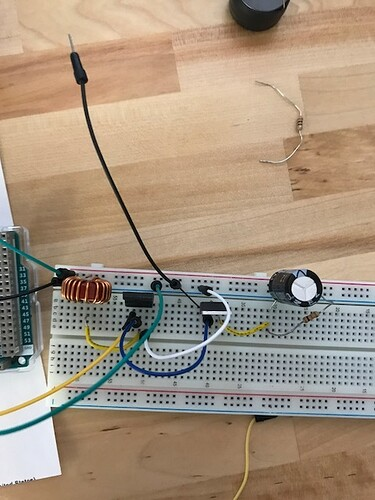
Breadboard prototype of the 5V → 15V boost converter.
Project Progress
Schematic & Simulation
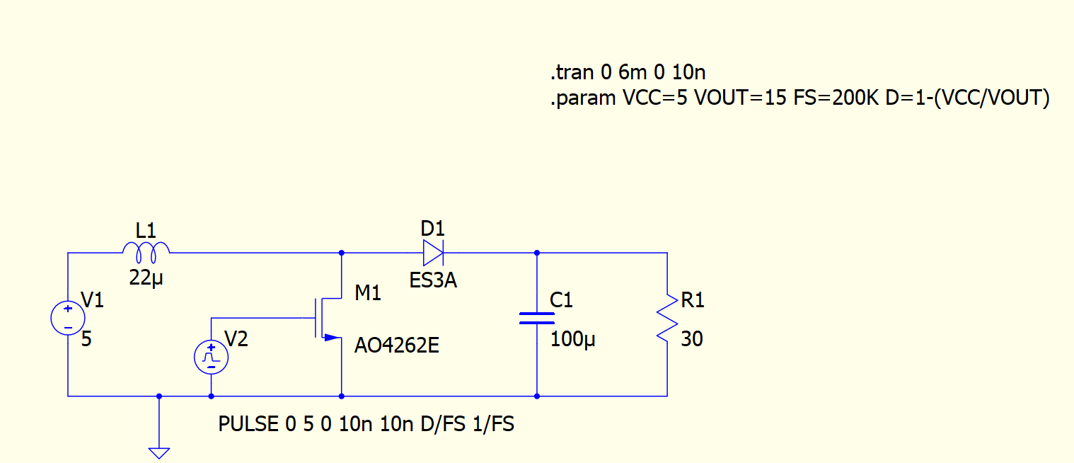
QSPICE schematic showing the 22µH inductor, AO4262E MOSFET, ES3A diode, 100µF capacitor, and 30Ω load.
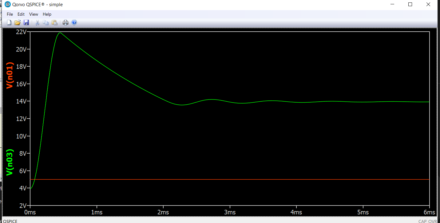
Simulation: output voltage ramps up from 5V, overshoots near ~22V, then settles close to the 15V target.
The simulation predicted a noticeable startup overshoot followed by a decaying ripple as the output settled. When I tested the real circuit, I observed a very similar shape on the oscilloscope, which gave me confidence that the model and component choices were reasonable.
Project Successes & Failures
Successes
- Successfully boosted 5V to approximately 15V on the bench.
- Simulation waveforms matched real hardware behavior (overshoot + settling).
- Component ratings were chosen correctly; no devices were overstressed.
- Demonstrated clear relationship between duty cycle and output voltage.
Roadblocks & Failures
- Overshoot: Initially saw a higher-than-expected peak voltage. This led me to think about soft-start and ramping duty cycle more gently.
- Ripple and ringing: Breadboard parasitics and long leads introduced ringing that was not as strong in simulation, highlighting layout as a key next step.
- Diode losses: The ES3A’s forward drop reduces efficiency; in a next revision I’d test a Schottky diode designed for switching converters.
ECE Skills Gained
Technical / Power Skills
- Understanding the boost converter topology and duty-cycle equation.
- Selecting inductor, diode, MOSFET, and capacitor values based on ratings and ripple.
- Using QSPICE to run transient simulations and interpret waveforms.
- Recognizing overshoot, ripple, and steady-state behavior on both plots and scope captures.
Practical Lab Skills
- Breadboarding a switching converter safely.
- Using an oscilloscope to measure output voltage vs. time.
- Debugging issues caused by parasitic inductance/Capacitance in wiring.
- Documenting results clearly with annotated screenshots and photos.
Final Thoughts & Future Work
Overall, this Discovery Project made power electronics feel much more concrete. Instead of just seeing the boost converter equation in a slide, I watched the inductor current ramp, the diode conduct, and the output voltage settle into place. It also showed me how important layout, parasitics, and component selection are if I ever want to ship a design instead of just simulating it.
This experience strengthened my interest in the Power & Electronics side of ECE. In the future, I’d like to design a PCB version of this converter, add proper feedback regulation, and measure real efficiency across load conditions. That would turn this Discovery Project into a stepping stone for more advanced converter designs.